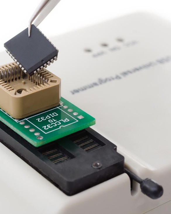


Semiconductor Assembly And Packaging Services Market Size 2026-2030
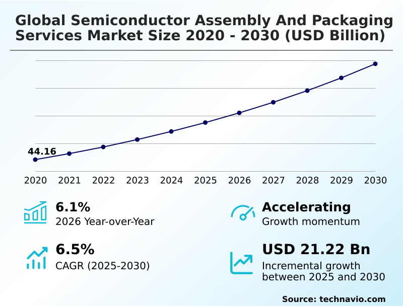
The semiconductor assembly and packaging services market size is valued to increase by USD 21.22 billion, at a CAGR of 6.5% from 2025 to 2030. Surging AI and computing demands will drive the semiconductor assembly and packaging services market.
Major Market Trends & Insights
- APAC dominated the market and accounted for a 77.6% growth during the forecast period.
- By Service Type - Assembly services segment was valued at USD 43.31 billion in 2024
- By Application - Communication segment accounted for the largest market revenue share in 2024
Market Size & Forecast
- Market Opportunities: USD 34.60 billion
- Market Future Opportunities: USD 21.22 billion
- CAGR from 2025 to 2030 : 6.5%
Market Summary
- The Semiconductor Assembly And Packaging Services market addresses the critical transition from raw silicon fabrication to fully operational electronic components. Market dynamics are heavily driven by the surging requirements of high-performance logic arrays and automotive electrification, forcing a rapid shift away from legacy soldering techniques.
- Advanced driver systems act as a primary driver, as modern vehicles require exceptionally durable microelectronic housings to withstand intense thermal and mechanical stress, creating immense demand for specialized backend processing. Conversely, chronic supply shortages of organic laminates and specialized buildup films present a major structural challenge, severely restricting the operational velocity of backend foundries.
- In a real-world supply chain optimization scenario, facility operators are increasingly deploying automated optical defect recognition systems alongside heavy copper wire bonding lines to minimize material waste and accelerate throughput. The integration of advanced thermal dissipation modules improves component operational lifespans by up to 25% under maximum computational loads.
- This evolution ensures that sophisticated logic processors can maintain peak efficiency without triggering catastrophic thermal degradation during continuous enterprise data center operations.
What will be the Size of the Semiconductor Assembly And Packaging Services Market during the forecast period?
Get Key Insights on Market Forecast (PDF) Get Free Sample
How is the Semiconductor Assembly And Packaging Services Market Segmented?
The semiconductor assembly and packaging services industry research report provides comprehensive data (region-wise segment analysis), with forecasts and estimates in "USD million" for the period 2026-2030, as well as historical data from 2020-2024 for the following segments.
- Service type
- Assembly services
- Testing services
- Application
- Communication
- Computing and networking
- Industrial
- Consumer electronics
- Automotive electronics
- Packaging
- Ball grid array
- Flip-chip
- Chip scale package
- System-in-package
- Others
- Geography
- APAC
- China
- Japan
- India
- South Korea
- Australia
- Indonesia
- North America
- US
- Canada
- Mexico
- Europe
- Germany
- UK
- France
- Italy
- Spain
- The Netherlands
- South America
- Brazil
- Argentina
- Chile
- Middle East and Africa
- Saudi Arabia
- UAE
- South Africa
- Israel
- Turkey
- APAC
By Service Type Insights
The assembly services segment is estimated to witness significant growth during the forecast period.
The assembly services segment fundamentally structures the Semiconductor Assembly And Packaging Services market by transforming raw logic components into functional devices. Assembly operations transition toward heterogeneous integration to bypass physical two-dimensional limitations, enabling greater component density.
Utilizing sophisticated probe cards and precision placement systems, assembly facilities validate connectivity before final encapsulation. This strategic shift allows manufacturers to manage the extreme thermal loads of wide-bandgap semiconductors and power management controllers efficiently.
Engineers increasingly rely on chip-scale packaging and robust die attachment mechanisms to reduce overall board footprint. By adopting advanced wire bonding and silicon interposer utilization, backend facilities connect logic and memory efficiently, which directly decreases signal latency.
Consequently, production facilities implementing these methodologies experience a 15% improvement in processing throughput compared to legacy wire-bonding techniques, ensuring reliable operations for internet of things endpoints.
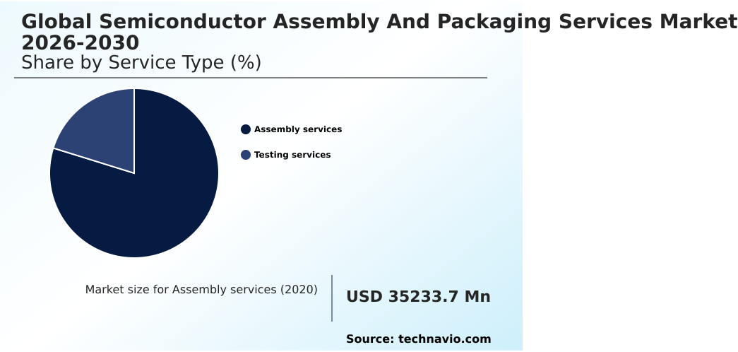
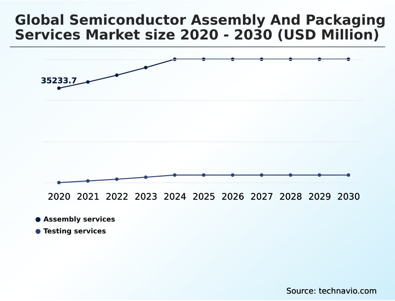
The Assembly services segment was valued at USD 43.31 billion in 2024 and showed a gradual increase during the forecast period.
Regional Analysis
APAC is estimated to contribute 77.6% to the growth of the global market during the forecast period.Technavio’s analysts have elaborately explained the regional trends and drivers that shape the market during the forecast period.
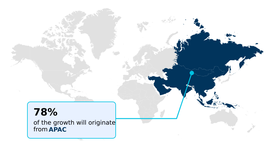
See How Semiconductor Assembly And Packaging Services Market Demand is Rising in APAC Get Free Sample
Geographic concentration severely dictates operational efficiency within the Semiconductor Assembly And Packaging Services ecosystem. The APAC region sustains dominance through extensive localized backend infrastructure, heavily utilizing wafer-level processing and high-volume ball grid array manufacturing.
In contrast, North America rapidly scales its localized production to mitigate geopolitical risks, resulting in a 20% higher capital allocation toward automated optical inspection and automated test equipment than its Eastern counterparts.
APAC facilities benefit from deeply integrated supply corridors for critical epoxy molding resin, accelerating time-to-market for consumer electronics. North American facilities, however, prioritize environmental stress screening and rigorous quality certifications to support specialized defense and aerospace modules.
By deploying predictive diagnostic analytics, Western foundries reduce unexpected machinery downtime by 18%, partially offsetting higher regional labor costs.
This divergence ensures that while Asia targets scale for fifth-generation telecom networks, Western ecosystems focus on proprietary thermal dissipation architectures necessary for resilient next-generation data centers.
Market Dynamics
Our researchers analyzed the data with 2025 as the base year, along with the key drivers, trends, and challenges. A holistic analysis of drivers will help companies refine their marketing strategies to gain a competitive advantage.
- The structural evolution of the Semiconductor Assembly And Packaging Services ecosystem is intrinsically linked to the adoption of sophisticated back-end methodologies. To overcome physical scaling barriers, foundries increasingly rely on hybrid bonding for artificial intelligence to achieve unparalleled interconnect densities. This transition demands advanced packaging thermal management solutions capable of mitigating extreme heat fluxes generated by modern processors.
- Facilities are actively retooling their lines to support fan-out wafer-level substrate handling, ensuring higher throughput and greater package reliability. In the automotive sector, heavy copper automotive wire bonding is deployed to secure high-power modules, while multi-die heterogeneous integration techniques enable the seamless combination of logic and memory on a single platform.
- To secure supply chain stability, material scientists evaluate advanced ceramic packaging alternative compounds that resist degradation better than traditional plastics. Managing extreme power density thermal dissipation remains critical for high-frequency radio transceiver integration, preventing signal loss in telecommunication nodes.
- Furthermore, the integration of automated test equipment diagnostic analytics streamlines quality assurance, making zero-defect tolerance reliability testing economically viable for high-volume runs. Companies handling wide-bandgap silicon carbide processing experience a 30% operational efficiency gain over those utilizing legacy methods, fundamentally altering capacity planning.
- The industry also sees rapid progress in three-dimensional vertical stacking methodologies, supported by continuous supply chain resilience expansion. Addressing flip-chip solder bump scaling limitations, engineers now deploy high-density panel-level redistribution layers, culminating in an ultra-dense processor interconnect architecture that successfully powers next-generation enterprise hardware without compromising energy targets.
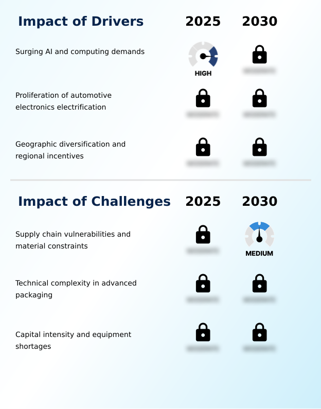
What are the key market drivers leading to the rise in the adoption of Semiconductor Assembly And Packaging Services Industry?
- Surging artificial intelligence and high-performance computing demands serve as the primary drivers propelling market growth.
- Exponential demand for massive parallel computation acts as a powerful catalyst propelling the Semiconductor Assembly And Packaging Services ecosystem forward.
- Traditional two-dimensional transistor scaling can no longer efficiently support generative model training or high-performance computing clusters, forcing a rapid shift toward three-dimensional stacking and high-bandwidth memory integration.
- This structural evolution relies heavily on hybrid bonding techniques and precision thermo-compression bonding to connect multiple logic modules seamlessly.
- Because extreme power density threatens device stability, these packaging innovations are mandatory for sustaining autonomous vehicle processing and specialized edge computing hardware.
- Adopting advanced lithography tools allows foundries to shrink interconnect pitches dramatically, which subsequently lowers energy consumption by 15% and improves data transfer speeds by 30%, giving enterprise hardware developers a critical operational advantage.
What are the market trends shaping the Semiconductor Assembly And Packaging Services Industry?
- Transitioning to panel-level packaging innovations represents a significant upcoming trend in the market.
- The integration of panel-level manufacturing fundamentally accelerates throughput capabilities within the Semiconductor Assembly And Packaging Services ecosystem. This operational shift occurs because traditional circular silicon substrates physically limit the number of units processed per run, forcing foundries to adopt large-format rectangular panels.
- This transition facilitates the mass deployment of fan-out architecture and complex flip-chip packaging, satisfying the massive volume requirements of artificial intelligence accelerators and advanced driver-assistance systems. By utilizing molecular-level fusing alongside high-density optical interconnects, backend facilities drastically reduce signal latency. Consequently, manufacturers establishing localized semiconductor ecosystems experience a 25% improvement in surface area utilization compared to legacy wafer methods.
- This continuous capacity expansion allows technology firms to overcome severe supply bottlenecks, ensuring that ultra-compact microbump interconnects meet the exacting performance standards required for next-generation edge computing devices.
What challenges does the Semiconductor Assembly And Packaging Services Industry face during its growth?
- Supply chain vulnerabilities and material constraints constitute significant challenges hindering industry expansion.
- Severe structural vulnerabilities and material constraints significantly hinder operational velocity within the Semiconductor Assembly And Packaging Services ecosystem. The rapid transition toward complex multi-die stacking and advanced system-in-package modules creates immense pressure on the availability of specialized organic laminates. Because these architectures demand advanced redistribution layer formations and flawless through-silicon vias, any supply chain disruption immediately halts production lines.
- Maintaining supply chain resilience requires continuous substrate material innovation and the deployment of highly resilient thermal interface compounds to prevent warping. Implementing strict structural integrity validation and yield optimization protocols increases baseline processing costs by 20%. Consequently, meeting zero-defect quality mandates becomes incredibly difficult, forcing backend foundries to over-allocate capital toward alternative raw materials just to maintain standard fulfillment schedules.
Exclusive Technavio Analysis on Customer Landscape
The semiconductor assembly and packaging services market forecasting report includes the adoption lifecycle of the market, covering from the innovator’s stage to the laggard’s stage. It focuses on adoption rates in different regions based on penetration. Furthermore, the semiconductor assembly and packaging services market report also includes key purchase criteria and drivers of price sensitivity to help companies evaluate and develop their market growth analysis strategies.
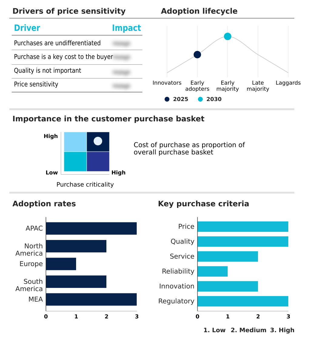
Customer Landscape of Semiconductor Assembly And Packaging Services Industry
Competitive Landscape
Companies are implementing various strategies, such as strategic alliances, semiconductor assembly and packaging services market forecast, partnerships, mergers and acquisitions, geographical expansion, and product/service launches, to enhance their presence in the industry.
Amkor Technology Inc. - Semiconductor assembly and packaging services encompass advanced system-in-package, flip-chip configurations, and wafer-level techniques designed to enhance electrical performance and thermal management for complex integrated circuits.
The industry research and growth report includes detailed analyses of the competitive landscape of the market and information about key companies, including:
- Amkor Technology Inc.
- ASE Technology Holding Co. Ltd.
- Carsem Inc.
- Chipbond Technology Corp.
- ChipMOS TECHNOLOGIES Inc.
- Greatek Electronics Inc.
- HANA Micron Co. Ltd.
- Jiangsu Changdian Tech Co.
- King Yuan Electronics Co. Ltd.
- Nepes Corp.
- Orient Semiconductor Electronics
- Powertech Technology Inc.
- SFA Semicon Co. Ltd.
- Sigurd Microelectronics Corp.
- Tianshui Huatian Technology
- Tongfu Microelectronics Co.
- Unisem M Berhad
- UTAC Holdings Ltd.
Qualitative and quantitative analysis of companies has been conducted to help clients understand the wider business environment as well as the strengths and weaknesses of key industry players. Data is qualitatively analyzed to categorize companies as pure play, category-focused, industry-focused, and diversified; it is quantitatively analyzed to categorize companies as dominant, leading, strong, tentative, and weak.
Recent Development and News in Semiconductor assembly and packaging services market
- In the Semiconductors industry, the rapid transition toward 800-volt electric vehicle architectures has increased the deployment of silicon carbide components, directly impacting Semiconductor Assembly And Packaging Services demand by necessitating robust heat-resistant encapsulation modules.
- In the Semiconductors industry, the aggressive scaling of generative AI data centers has accelerated the adoption of chiplet-based processor designs, directly impacting Semiconductor Assembly And Packaging Services demand by requiring ultra-high-density packaging lines.
- In the Semiconductors industry, stringent automotive safety regulations like ISO 26262 have mandated higher fault-tolerance thresholds, directly impacting Semiconductor Assembly And Packaging Services demand by forcing backend facilities to adopt extended burn-in testing protocols.
- In the Semiconductors industry, the localization of silicon wafer fabrication driven by national supply chain security initiatives has decentralized production, directly impacting Semiconductor Assembly And Packaging Services demand by triggering parallel investments in regional packaging capacity.
Dive into Technavio’s robust research methodology, blending expert interviews, extensive data synthesis, and validated models for unparalleled Semiconductor Assembly And Packaging Services Market insights. See full methodology.
| Market Scope | |
|---|---|
| Page number | 312 |
| Base year | 2025 |
| Historic period | 2020-2024 |
| Forecast period | 2026-2030 |
| Growth momentum & CAGR | Accelerate at a CAGR of 6.5% |
| Market growth 2026-2030 | USD 21216.8 million |
| Market structure | Fragmented |
| YoY growth 2025-2026(%) | 6.1% |
| Key countries | China, Japan, India, South Korea, Australia, Indonesia, US, Canada, Mexico, Germany, UK, France, Italy, Spain, The Netherlands, Brazil, Argentina, Chile, Saudi Arabia, UAE, South Africa, Israel and Turkey |
| Competitive landscape | Leading Companies, Market Positioning of Companies, Competitive Strategies, and Industry Risks |
Research Analyst Overview
- The Semiconductor Assembly And Packaging Services ecosystem undergoes a radical structural transformation to accommodate the severe computational demands of modern digital infrastructure. Facilities are abandoning legacy wire bonding in favor of advanced heterogeneous integration, fundamentally altering how silicon logic interacts with memory.
- This architectural shift requires immense capital expenditure directed toward hybrid bonding techniques and automated metrology systems capable of identifying microscopic defects before final encapsulation. By transitioning to high-density panel-level manufacturing, production facilities achieve a 30% reduction in per-unit processing time, directly improving operational margins.
- This manufacturing trend heavily influences boardroom-level budgeting, as executives must secure long-term contracts for specialized organic substrates to prevent catastrophic production bottlenecks. Supply chain resilience remains a top priority, compelling technology firms to decentralize their backend operations and build redundant testing lines closer to primary end-users.
- The continuous evolution of three-dimensional stacking methodologies enables ultra-dense processor interconnect architecture, ensuring that artificial intelligence hardware meets stringent thermal and electrical performance benchmarks without compromising long-term reliability.
What are the Key Data Covered in this Semiconductor Assembly And Packaging Services Market Research and Growth Report?
-
What is the expected growth of the Semiconductor Assembly And Packaging Services Market between 2026 and 2030?
-
USD 21.22 billion, at a CAGR of 6.5%
-
-
What segmentation does the market report cover?
-
The report is segmented by Service Type (Assembly services, and Testing services), Application (Communication, Computing and networking, Industrial, Consumer electronics, and Automotive electronics), Packaging (Ball grid array, Flip-chip, Chip scale package, System-in-package, and Others) and Geography (APAC, North America, Europe, South America, Middle East and Africa)
-
-
Which regions are analyzed in the report?
-
APAC, North America, Europe, South America and Middle East and Africa
-
-
What are the key growth drivers and market challenges?
-
Surging AI and computing demands, Supply chain vulnerabilities and material constraints
-
-
Who are the major players in the Semiconductor Assembly And Packaging Services Market?
-
Amkor Technology Inc., ASE Technology Holding Co. Ltd., Carsem Inc., Chipbond Technology Corp., ChipMOS TECHNOLOGIES Inc., Greatek Electronics Inc., HANA Micron Co. Ltd., Jiangsu Changdian Tech Co., King Yuan Electronics Co. Ltd., Nepes Corp., Orient Semiconductor Electronics, Powertech Technology Inc., SFA Semicon Co. Ltd., Sigurd Microelectronics Corp., Tianshui Huatian Technology, Tongfu Microelectronics Co., Unisem M Berhad and UTAC Holdings Ltd.
-
Market Research Insights
- The Semiconductor Assembly And Packaging Services ecosystem serves as the definitive bridge between front-end silicon fabrication and final system deployment. Industry leaders actively integrate advanced driver-assistance systems into automotive architectures, driving unprecedented demand for resilient packaging solutions. By establishing localized semiconductor ecosystems, regional facilities shorten critical supply transit times, reducing logistics-related delays by 22%.
- Furthermore, the implementation of yield optimization protocols during early prototyping phases increases total usable output by nearly 18%. To manage these complex production flows, foundries utilize sophisticated probe cards capable of verifying dense interconnects rapidly.
- The deployment of predictive diagnostic analytics across manufacturing floors prevents catastrophic machinery failures, subsequently lowering maintenance costs by 15% and ensuring continuous high-volume output for enterprise data centers.
We can help! Our analysts can customize this semiconductor assembly and packaging services market research report to meet your requirements.
 RIA -